Team Members
- Nicolas Casazzone
- Alicia Coto
- Raul Pacheco
Materials
- Arduino Uno
- FPGA DE0_nano
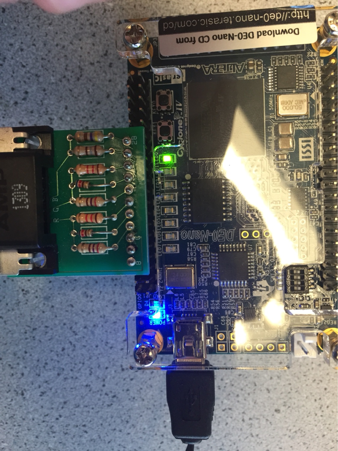
- 8-bit DAC Connector
- VGA Cable
- Various Resistors
- 2x Switches
Deciding Resistor Values for the 8-bit DAC
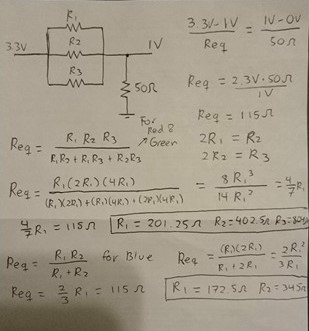
To encode colors to the screen, we needed to use an 8-bit DAC (Digital to Analog Converter), which is shown in the image below. This DAC uses 3 of the bits to encode the values for the color red, 3 bits to encode green, and 2 bits to encode blue. This DAC connects to 8 pins on the FPGA that then feeds through 8 different resistors. From there, the group of wires for each color combine to produce a voltage between 0 and 1 V. The resistors step down the voltage from 3.3 volts to different voltages. The resistor values for each resistor in a color group must correspond with different voltage step downs so that a range of out voltages can be attained. For red and green, since they are comprised of 3 bits, 8 different colors should be producible. This means that 8 different voltages between 0 and 1V should be achieved, each 1/7 of a volt apart.
From the picture above, each color indicated by R, G, B has resistors in parallel along with the VGA cable having a 50Ω resistance in series. The voltage of each color pin needs to sum to a total of 1V with each pin representing a bit. The most significant bit is twice the voltage of the second most significant bit, four times the voltage of the third most significant bit, and so on. The voltage of each color branch is 4/7V, 2/7V, and 1/7V respectively to the most significant bit order. Below is our worked out solution to finding the resistor values for the DAC. To keep the current across the resistors the same, the resistor for the most significant bit would be have twice the resistance of the second significant bit, and so on, just like the voltages. Hence the assumption of 2R1=R2, and 2R2=R3.
Drawing to the Screen
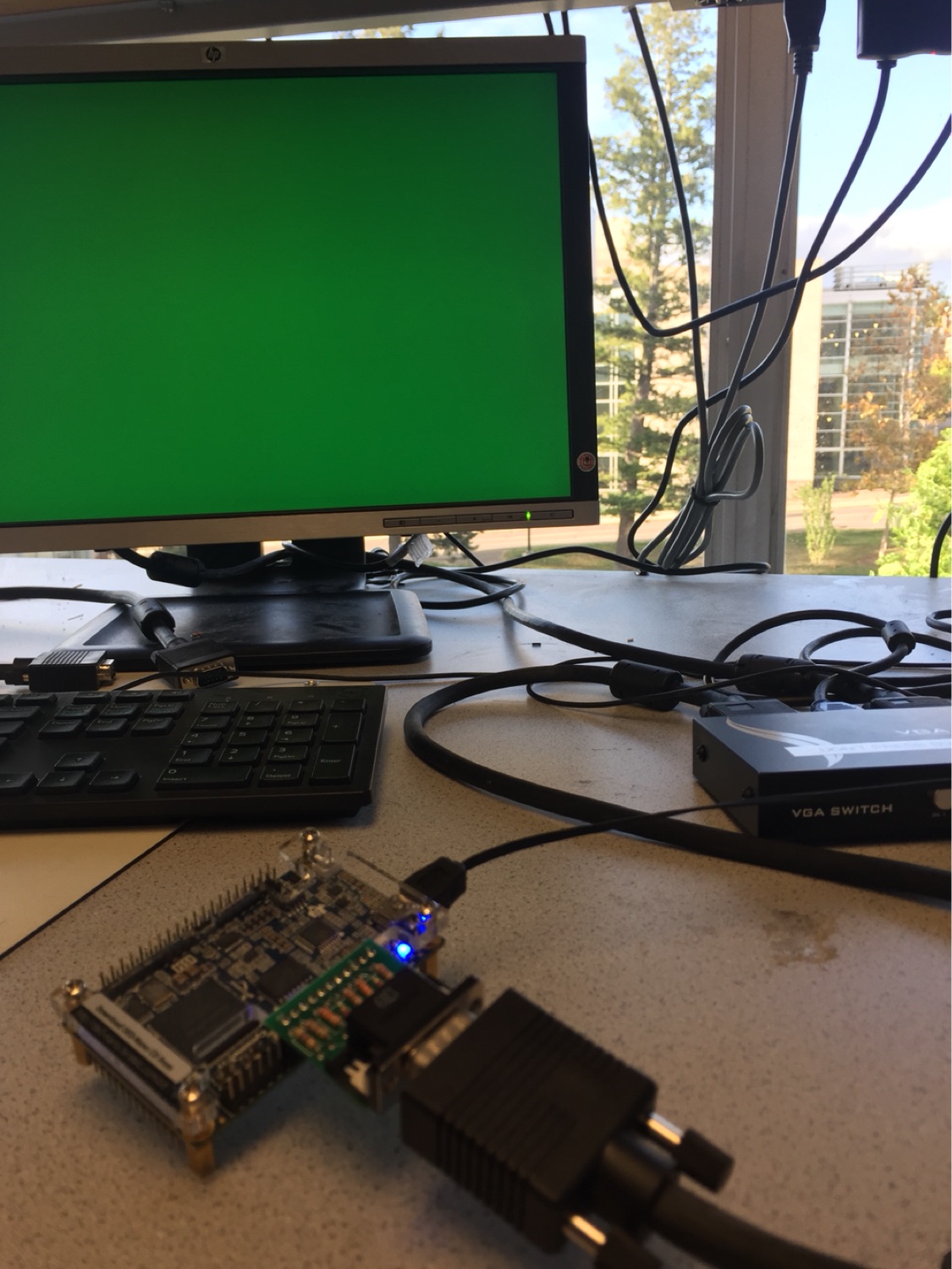
We were given a VGA module written in verilog that is used to write values to the pixels on our screen. The module works with our main module by giving it an x and y coordinate (PIXEL_COORD_X and PIXEL_COORD_) that correspond to the position of a pixel on the screen. In the main module, we write a color to the pixel in an 8 bit variable, PIXEL_COLOR, which is then sent by the VGA driver to the DAC and eventually displays the color on the screen. The first 3 bits of PIXEL_COLOR coorespond to red, the next 3 to green and the last two to blue. The VGA module incrememnts through each pixel on the screen by continuously outputting the next pixel coordinates. In the image below, every pixel was assigned to green (8'b000_111_00).
External Inputs to the Screen
Before using external imputs we first wanted to create a 2x2 grid on the screen. The code below shows the logic that we used. We used a 2x2 matrix, my_grid of 8 bit values to store the colors of each sqare in the grid. The 1 bit regs, newx and newy, convert PIXEL_COORD_X and PIXEL_COORD_Y into values that correspond to each box in the 2x2 grid. If x is 0, we are assigning to the column on the left; if x is 1, we are assigning to the column on the right. If y is 0 we are assigning to the top row, if y is 1, we are assigning to the bottom row. We made our grid 200 pixels by 200 pixels so we added a case for if the pixel was located beyond our grid. If it was, it was simply assigned the color black, which is 8 zeros. This allows us to assign PIXEL_COLOR to the value stored in my_grid[x][y]. The always block used with an asterix ensures that the block runs whenever any input signal changes.
                         wire[7:0] my_grid[1:0][1:0];

                         reg newx;
                         reg newy;

                         assign my_grid[0][0] = 8'b000_000_11;
                         assign my_grid[1][0] = 8'b111_111_11;
                         assign my_grid[0][1] = 8'b111_111_11;
                         assign my_grid[1][1] = 8'b000_000_11;

                        always @ (*) begin

                            newx = PIXEL_COORD_X/10'd100;
                            newy = PIXEL_COORD_Y/10'd100;
                            if (PIXEL_COORD_X > 199 | PIXEL_COORD_Y > 199) begin
                                PIXEL_COLOR = 8'd0;
                            end
                            else begin
                                PIXEL_COLOR = my_grid[newx][newy];
                            end
                        end
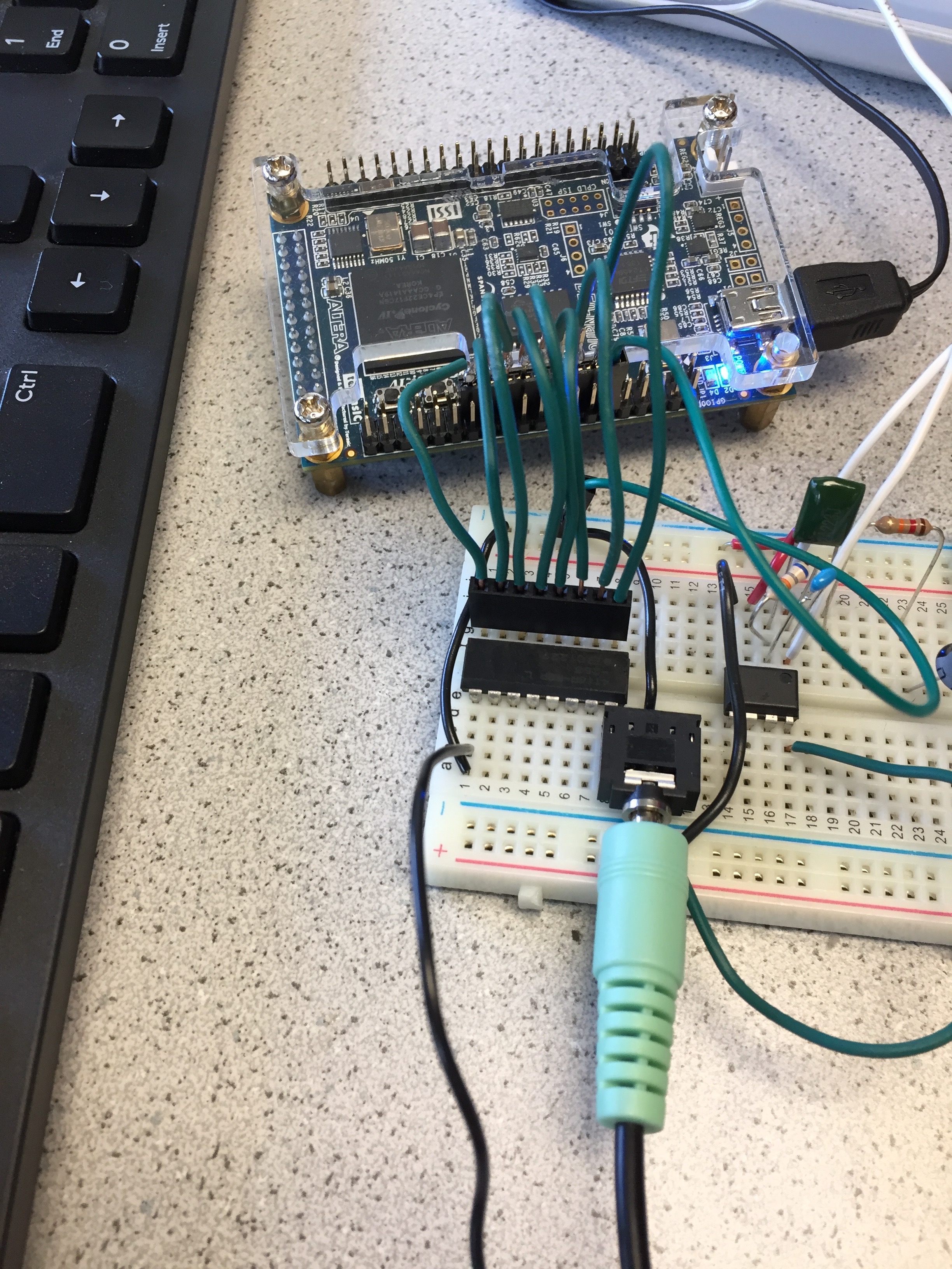
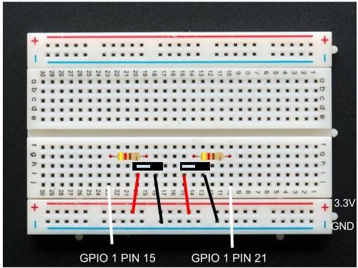
In order to demonstrate an external input controlling our 2x2 grid, we implemented two switches to provide combinations for our four possible grid outcomes. The switch has 3 pins, only two of which are connected at a time. We made the middle pin the signal pin with the two other pins being 3.3 volts and ground. When the switch is flipped, the signal pin flips between 0 and 3.3 volts. This is read as a 0 or 1 by the FPGA. The following image shows how we wired the switches to pins on the FPGA.
Each different switch position combination corresponds with a blue box being in one of the 4 quadrants of our grid. The table below shows the different outputs based on the switch position.
| Switch One | Switch Two | Blue Quadrant |
|---|---|---|
| 0 | 0 | Top Left |
| 1 | 0 | Top Right |
| 0 | 1 | Bottom Left |
| 1 | 1 | Bottom Right |
Below is our code which uses the switch inputs to determine the color of each quadrant of my grid. Pin1 and pin2 were assigned to the GPIO pin that the switch signal was plugged into on the FPGA.
                         always @ (*) begin
                            if(pin1 == 0 & pin2 == 0)begin
                                 my_grid[0][0] <= 8'b000_000_11;
                                 my_grid[1][0] <= 8'b111_111_11;
                                 my_grid[0][1] <= 8'b111_111_11;
                                 my_grid[1][1] <= 8'b111_111_11;
                             end
                             else if(pin1 == 1 & pin2 == 0)begin
                                 my_grid[0][0] <= 8'b111_111_11;
                                 my_grid[1][0] <= 8'b000_000_11;
                                 my_grid[0][1] <= 8'b111_111_11;
                                 my_grid[1][1] <= 8'b111_111_11;
                             end
                             else if(pin1 == 0 & pin2 == 1)begin
                                 my_grid[0][0] <= 8'b111_111_11;
                                 my_grid[1][0] <= 8'b111_111_11;
                                 my_grid[0][1] <= 8'b000_000_11;
                                 my_grid[1][1] <= 8'b111_111_11;
                             end
                             else begin
                                 my_grid[0][0] <= 8'b111_111_11;
                                 my_grid[1][0] <= 8'b111_111_11;
                                 my_grid[0][1] <= 8'b111_111_11;
                                 my_grid[1][1] <= 8'b000_000_11;
                             end


                            newx = PIXEL_COORD_X/10'd100;
                            newy = PIXEL_COORD_Y/10'd100;
                            if (PIXEL_COORD_X > 199 | PIXEL_COORD_Y > 199) begin
                                PIXEL_COLOR = 8'd0;
                            end
                            else begin

                                PIXEL_COLOR = my_grid[newx][newy];
                            end
                        end
Below is a video of our switches in action!